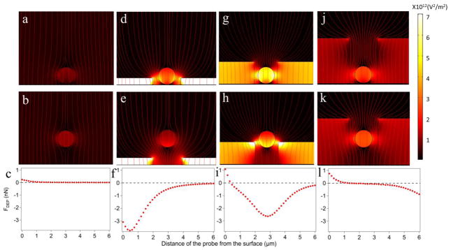
Figure 6.
Electric field distributions in Geometry A (a–c), Geometry B (d–f), and Geometry C (g–l) for a 3 μm diameter probe at 50 nm (a, d, g, and j) and 3 μm (b, e, h, and k) above the surface of the electrode. When close to the surface, the probe is pulled up (FDEP>0) by the positive DEP force in (a), (g), and (j), and by the negative DEP in (d). The red streamlines represent the electric field. The surface plots are E2 and all six graphs share the same scale. (c), (f), (i), and (l) The DEP forces versus distance from the surface when the 3 μm probe is moving away from the electrode.

