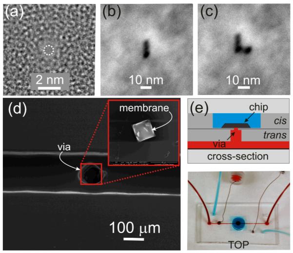
FIGURE 1. Nanopores sputtered with sub-nanometer precision in small area membranes embedded in microfluidics.

(a) TEM micrograph of a nanopore 0.7×0.9 nm in cross-section. (b,c) Scanning TEM (STEM) micrograph of a slit and an “L” pattern respectively, indicating stability of the beam (<1 nm drift/30 min.) (d) Scanning Electron Microscopy (SEM) of a silicon chip with a Si3N4 membrane on it (inset) bonded to a PDMS microfluidic at the top of a 75 μm via in the middle of a 150 μm microchannel.(e) (top) Schematic showing a magnified view of a horizontal cross-section through the device and (bottom) optical micrograph showing the top view of a PDMS microfluidic with two channels: one above (blue) and the other below (red) the silicon membrane.
