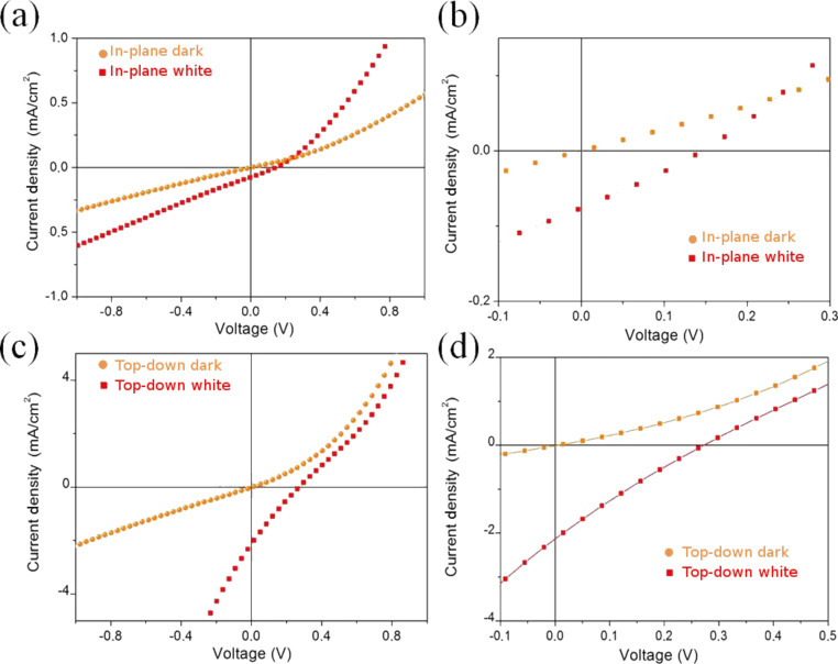
Figure 10.
J–V characteristics acquired in the dark and under illumination by white light. (a) In the in-plane geometry: Voc = 0.2 V, Jsc = 0.09 mA/cm2. In the third and fourth quadrant the J–V curve is almost linear. This could be due to the presence of parasitic resistances, which lower the performance of the device. An inhomogeneous MWCNT film, in which all the MWCNTs are not in good contact with each other, could be the cause of such a high resistance. (b) Detail of (a) in the most meaningful zone, i.e., in the fourth quadrant of the J–V characteristic. (c) Top-down geometry: Voc = 0.25 V, Jsc = 2.2 mA/cm2. Under illumination, the J–V curve line shape exhibits the behaviour of a double diode: beyond the MWCNT–Si Schottky junction, the second one is formed at the back contact between Si and Al, i.e., a hint of a non-ohmic contact. (d) Detail of (c) in the most meaningful zone, i.e., in the fourth quadrant of the J–V characteristic.

