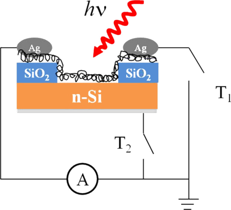
Figure 8.
Scheme of the photovoltaic device. The Schottky junction between the Si and the MWCNT film is the photoactive junction. Steps of SiO2 (300 nm) are used to avoid a short-circuit forming between the silver paint (top electrode) and the silicon substrate. The back contact is made of aluminium. In the in-plane geometry, the switch T1 is on and T2 is off; and vice versa in the top-down configuration. As a result, the photocurrent is collected at the MWCNT film in the former case, and at the MWCNTs and Si (back contact) in the latter.

