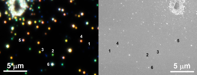
Figure 2. Dark-field microscope (a) and top-view scanning electron microscope (SEM) (b) images of the same area on a silicon wafer ablated by a femtosecond laser.
Microscope image is inverted in horizontal direction relative to that of the SEM. Selected nanoparticles are marked by corresponding numbers 1 to 6 in both figures.

