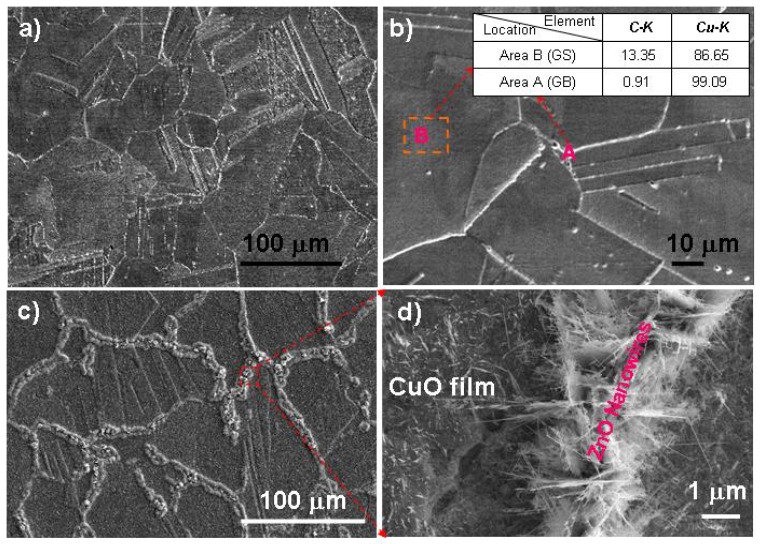
Figure 20.
(a,b) are respectively, a low-magnification and a high-magnification SEM image of metallographically etched Cu70Zn30 polycrystalline substrate revealing clearly the GB networks. Inset in (b) is an EDXS composition table revealing the Cu-rich GS after etching process; (c) A typical low-magnification top view SEM image of ZnO nanowires/CuO film heterojunction network after 4-h ambient oxidation at 500 °C; (d) A zoom-in top view SEM image showing the distinct growth morphology in the GS region (CuO nanofilms) and GB region (ZnO nanowires).

