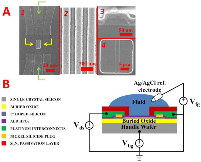
Figure 2.
Scanning electron micrographs of the silicon nanowires are in A. Image 1 shows an overview of the nanowire sensing area, with the source-drain metal leads (green arrows) and release window (yellow arrows) highlighted. A high magnification top-down image of the nanowires is shown in 2. A cross-sectional image of a nanowire is in 3 while a top down image a nanoplate is in 4. A horizontal cross sectional schematic of sensing setup is represented in B. The relevant structures are color coded to the left, with an example electrical measurement setup for the source drain (Vds), fluid gate (Vfg), and back gate (Vbg).

