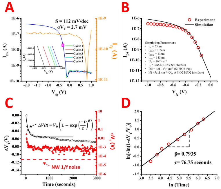
Figure 3.
Representative source-drain current verse fluid gate voltage for a nanowire is shown in A. The nanowires were swept for 5 cycles with the fluid gate leakage also measure (right side of graph) and an enlarged view of the curve repeatability is inset in A. The numerical simulation (black line) of the average of the experimental transfer curves in A (red circles) is shown in B with the simulation parameters (inset). The change in the threshold voltage (left side) and standard deviation in threshold (right side) versus time for a nanowire is in C. The equation for modeling the gate voltage instability is inset in C, with the fit to the experimental data represented as the black line. The theoretically estimated low frequency voltage noise is represented as a dashed red line. The experimental ΔVt data in C was rearranged according to the equation in C to extract the time constant and dispersion parameter. The natural log of the rearrangement is plotted in D versus the natural log of the time (red circles), with the linear fit to the data (black line) and the extracted parameters (inset).

