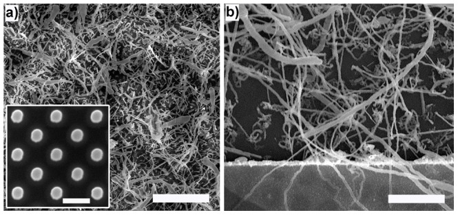
Figure 1. Device Fabrication.

(a) SEM image of complex Ag networks (scale bar = 10 µm) produced by reaction of aqueous AgNO3 (50 mM) with (inset) lithographically patterned Cu seed posts (scale bar = 1 µm). (b) High resolution image of the functionalized Ag network at the device electrode interface (Pt) showing wire widths ranging from 100 nm to 3 µm (average <1 µm) and lengths extending from a few microns to almost a millimeter (scale bar = 700 nm).
