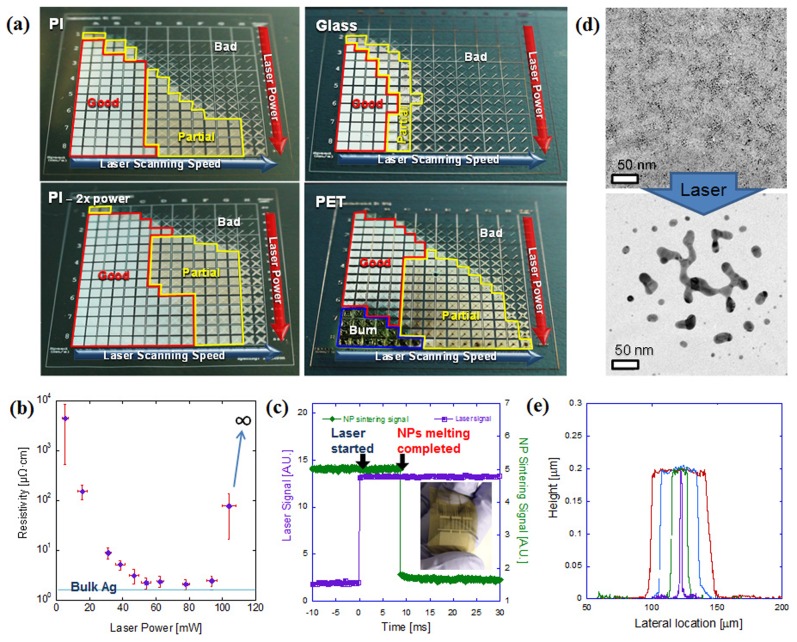
Figure 2. Process Characterization of Laser Induced Melting of Ag NP Ink During DDMP.
a, Combinatorial study for optimum laser power vs. laser scanning speed on PI (left top & bottom), glass (right top) PET(right bottom). Laser power and laser scanning speed in “Good” regimes (red boxes) were used for real process. Detailed laser scanning speed and laser power values can be found in Supporting Information (figure S2). The total size and unit box size for combinatorial study was 2 cm×2 cm and 1 mm×1 mm respectively. b, Resistivity change at various laser power. Blue line shows the resistivity value of bulk Ag (1.59 µΩ·cm) c, Process time characterization by transient resistance change measurement; time required for Ag NP melting (green) after laser irradiation (purple). Inset picture shows the Ag electrode patterns for process time measurement on a polymer substrate. d, TEM pictures of Ag NPs before (top) and after (bottom) laser irradiation. e, AFM cross sectional profiles of laser process Ag line patterns.

