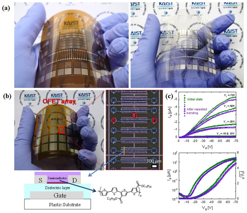
Figure 4. Large Area Flexible Electronics Demonstration through DDMP Process.
a, Single layer Ag micro patterns on PI(left) and PET(right) flexible substrates (4 inch wafer size). The pattern size varies from several microns to several centimeters. b, Multiple layer Ag micro patterning for OFET array demonstration on a flexible substrate. Right picture shows the magnified view of OFET arrays. Bottom picture shows the semiconducting polymer and cross sectional structure of the OFET. Letters “G”,”S”,”D” represent gate, source and drain respectively. c, Output (top graph) and transfer (bottom graph) characteristics of OFET before (green) and after (purple) cyclic bending test. Note that no significant OFET performance change was observed after 100,000 times bending.

