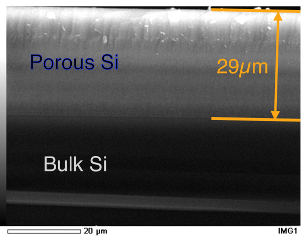
Figure 2.
Cross-section SEM image of a PSi sample for thickness measurement. The porous layer and the underlying bulk Si are indicated. The PSi external surface and the interface with the bulk Si substrate are indicated with the upper and lower orange lines, respectively. The measured thickness value is also shown.

