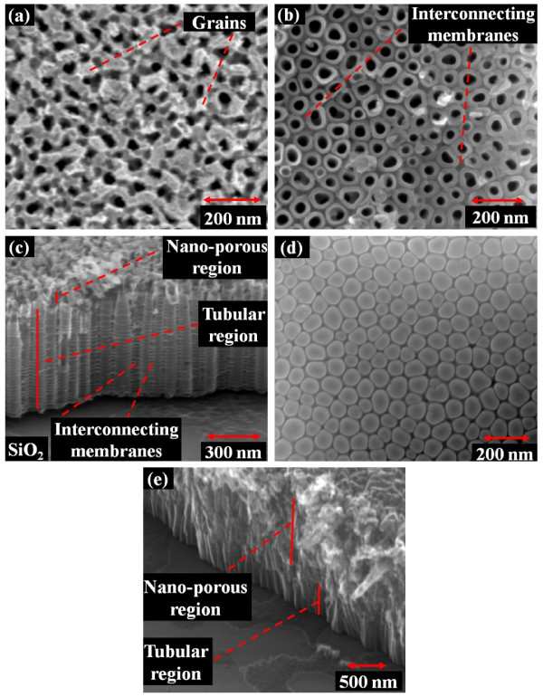
Figure 2.
SEM micrographs. The T-NT formed by anodization of 650-nm-thick, D.C.-sputtered Ti at 20 V for 1 h. (a) Top view of the T-NT. (b) Top view after milling about 400 nm of the T-NT top surface. (c) Side view showing the length and outer diameter of the tubes (imaged at 60° tilt). (d) Bottom of the tube after peeling from the wafer. (e) The increase in the nano-porous region due to the presence of thermally induced native TiO2 (1-μm-thick film).

