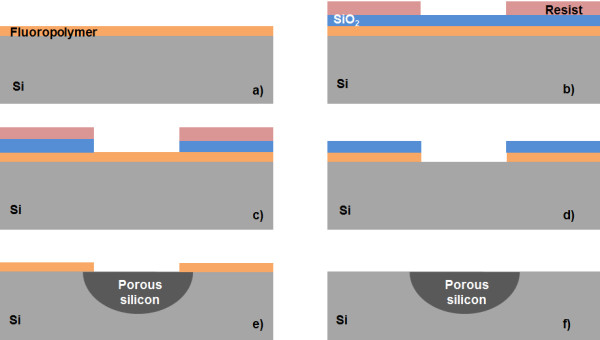
Figure 1.

Typical process used to fabricate the openings in the FP. (a) The FP is plasma-deposited. (b) A silicon dioxide layer is deposited by PECVD, and the photoresist is deposited by spin coating. The photoresist is patterned by photolithography. (c) The oxide is etched through the resist. (d) The FP is then etched through the oxide mask with O2 plasma that also removes the remaining resist. (e) The sample is anodized to form porous silicon; the oxide is etched during the anodization. (f) Finally, the FP is totally removed with O2 plasma.
