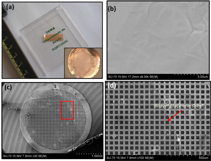
Figure 2. Optical and FESEM images of graphene prepared by HFTCVD.
(a) Large area as-deposited graphene film deposited on Cu substrate (inset shows optical image bilayer graphene transferred on Cu TEM grid). (b) Shows FESEM image for the as grown graphene films on Cu. (c) Shows FESEM image of BLG sheet on Cu grid. (d) Shows high magnification FESEM image for the area denoted in Fig. 2c by red line.

