Abstract
This Perspective describes how multi-scale plasmonic structures with two or more length scales (fine, medium, coarse) provide an experimental route for addressing the inverse problem. Specific near-field and far-field optical properties can be targeted and compiled into a plasmon resonance library by taking advantage of length scales spanning three orders of magnitude, from 1 nm to greater than 1000 nm, in a single particle. Examples of multi-scale 1D, 2D, and 3D gold structures created by nanofabrication tools and templates are discussed, and unexpected optical properties compared to those from their smaller counterparts are emphasized. One application of multi-scale particle dimers for surface-enhanced Raman spectroscopy is also described.
Keywords: Anisotropic nanoparticles, multi-scale particles, multipolar plasmon modes, gold nanoparticles
The ability to determine the geometry of a metallic nanoparticle (NP) based on its targeted optical properties is an inverse problem and a current challenge in plasmonics. By far, it is easier to make the nanostructure and then model the resulting near-field and far-field optical response. One reason for this difficulty is the same as to why noble metal NPs are so interesting in the first place: their localized surface plasmon (LSP) resonances can be tuned by tailoring the size, shape, and composition of the NP.1–3 The inverse problem becomes increasingly prohibitive to solve if we aim for a specific optical response by manipulating specific structural features within a single NP. For example, a particle with an average size much smaller than the wavelength of incident electromagnetic (EM) light (λEM) only supports dipolar resonances that weakly depend on size and shape.4 However, large particles with overall sizes that are comparable to or larger than λEM can support higher-order (e.g. quadrupolar, octupolar) plasmon modes that are sensitive to small changes in either size or shape.5–8 In this Perspective, we present the case that multi-scale NPs—structures with feature sizes that span three-orders of magnitude—offer a potential experimental solution to the inverse problem because they combine structure-function properties of both small and large metal particles.
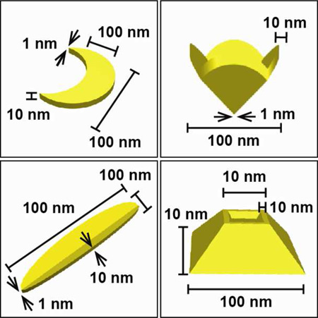
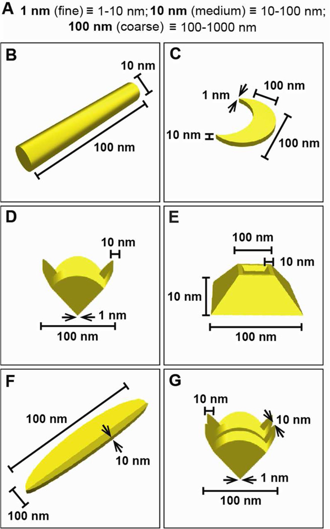
We first define three length scales that can describe distinct structural features within a multi-scale, anisotropic NP: (1) fine (1–10 nm), (2) medium (10–100 nm), and (3) coarse (> 100 nm) (Figure 1A). We made this division based on literature precedent, where NPs with a small radius of curvature or particles with sharp features (<10 nm) can produce high local electric field enhancements.9–11 The fine length-scale regime mostly determines the near-field properties. Additionally, changing the shell thickness (10–100 nm) of a dielectric core-metal shell NP can induce plasmon coupling between inner and outer shells, whose interaction is determined by shell thickness.12,13,14–16 Also, large metal particles with at least one dimension greater than 100 nm exhibit multipolar plasmon resonances.5–8 The coarse length-scale will have the greatest effect on far-field optical properties. Therefore, by combining these types of properties within a single, multi-scale NP, we can begin to determine the geometries necessary for a targeted optical response. To make this problem even more tractable, here we will focus on NPs constructed from a single material—gold—which in turn will define the wavelength range of interest, namely the visible and near-infrared regime.
Figure 1. Multi-scale Au Nanoparticles with Different Geometries.
(A) Definition of multi-scale particles with fine, medium, and coarse length scales also indicated in cartoons in (B–G). Nanofabrication approaches using templates can be used to generate (B) 1D nanorods (AAO template),6 (C) 2D nanocrescents (polystyrene bead template),30 (D) 3D nanopyramids (etched square pyramidal Si template),32 (E) 3D tipless pyramids (etched square pyramidal Si template),13 (F) 3D multi-scale particles with high aspect ratios (etched rectangular Si template),8 and (G) nanopyramidal dimers with an air gap (etched square pyramidal Si template).16
Although solution-based syntheses can produce a range of anisotropic NPs such as nanorods, bipyramids, and nanostars,17–20 such structures tend to be limited to two length scales: fine and medium. One exception is core-shell gold nanoshells,21 but since their overall shape is symmetric, we will exclude them from this discussion. Nanofabrication methods are an attractive approach not only for producing monodisperse particles reproducibly22–25 but also for controlling NP architecture at all three length-scale regimes (fine, medium, coarse), either independently or in combination as desired. In this Perspective, we will discuss the fabrication and characterization of multi-scale NPs with one-dimensional (1D) and two-dimensional (2D) architectures (Figures 1B–C). These anisotropic structures typically support at least two length scales. Next, we will describe three-dimensional (3D) structures in which specific structural features can be tuned in each of the three regimes (Figures 1D–G). Finally, we will highlight how multi-scale NPs can result in well-defined 3D hot spots by coupling specific features for applications such as surface-enhanced Raman spectroscopy (SERS).
Multi-scale Plasmonic NPs with Quasi-1D and 2D Architectures
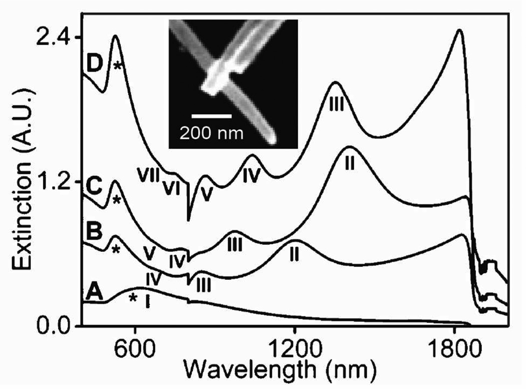
Nanofabrication approaches for creating multi-scale NPs relies on templates. For quasi-1D structures such as nanorods (Figure 1B), the templates are typically anodized aluminum oxide (AAO) membranes.6, 22, 26–28 Within the insulating channels (diameter d), conducting material is deposited by electrodeposition, and the length l of the rod is determined by the amount of time charge is applied in the process. Nanorods with fixed d = 85 nm and various l (96–1175 nm) showed multipolar plasmon resonances that shifted to longer wavelengths as the length or aspect ratio (AR) increased6 (Figure 2). Note that the number of higher-order modes within a fixed wavelength range also increased. Another noteworthy aspect of this multi-scale 1D NP is that the spectral position of the longitudinal dipole and quadrupole resonances of Au nanorods increased linearly with larger AR but increased nonlinearly with larger d (d = 35–100 nm, AR = 1–8).28 Thus, without the coarse length-scale features in the nanorods, only linear properties of the longitudinal dipole would have been observed, but which is expected based on lithographically defined nanorods at the fine length scale.29
Figure 2. Multi-scale 1D Nanorods Show Multipolar Plasmon Resonances.
The longitudinal dipole and quadrupole resonances of fabricated Au nanorods increased linearly with larger aspect ratios but increased nonlinearly with larger diameters. (inset) SEM image of Au rods. Labels A–D correspond to nanorod lengths of 96, 641, 735, and 1175 nm, respectively. Adapted with permission from ref. 6. © (2006) American Chemical Society.
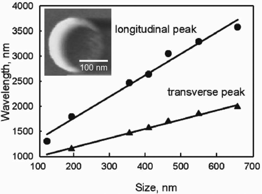
Templates for 2D structures are typically soft materials, such as patterned polymer resists, or hard materials, such as assembled monolayers of or isolated spherical beads. One example of a multi-scale 2D particle is a nanocrescent (Figure 1C) that can have tailorable dimensions, with diameter (d = 60–660 nm), thickness (t = 20–45 nm), and tip radius (< 10 nm).24, 30,31 The largest dimension is defined by the diameter of the polystyrene sphere template and the thickness by metal deposition. The separation between the two tips (gap distance (g)) can be controlled by the rotation angle between two sequential metal depositions. Au nanocrescents show transverse and longitudinal LSPs that red-shift linearly with increased d (Figure 3);30 the longitudinal resonances also shifted to longer wavelengths with decreased g.31 Not surprisingly, decreasing g increased coupling between the tips and can be used to maximize the local field enhancement,9 and strong coupling between the tips was observed when g < 10 nm. That small changes in g can affect both near-field and far-field optical responses points to the uniqueness of structures that support features over three orders of magnitude.
Figure 3. Multi-scale 2D Nanocrescent Particles show Longitudinal and Transverse Peaks.
These resonances red-shift linearly as the overall size of the particle increases as well as when the tip-tip distance decreases. (inset) SEM image of a Au nanocrescent. Adapted with permission from ref. 30 © (2007) American Chemical Society.
Multi-scale Plasmonic NPs with 3D Architectures
To fabricate 3D, multi-scale anisotropic particles, templates with 3D structure are necessary. We have designed one type of 3D template by anisotropically etching pyramidal pits into Si (100) wafers. The process to define the sizes of the Si pits and to transfer the patterns into Au (or any other material) is called PEEL (Phase-shifting photolithography, Etching, E-beam deposition, and Lift-off).25 This procedure is extremely flexible and not only can produce nanopyramidal shells (Figure 1D) with different shell thicknesses, materials, and shell sizes32 but can also generate nanopyramid derivatives, including tipless nanopyramids,13 multi-scale particles with different aspect ratios,8 and pyramidal shells with defined air gaps16 (Figures 1E–G).
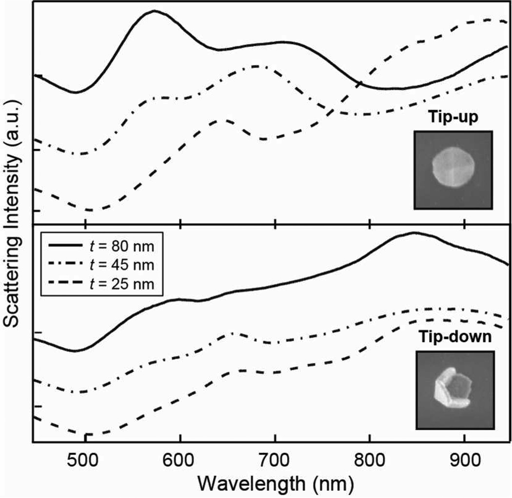
Au nanopyramids are intrinsically multi-scale in structure, with base diameters (db = 80 nm to >3000 nm), shell thicknesses (t > 10 nm), and tip radius (r = 2–10 nm).25, 32–34 db is determined by the photoresist post diameter in the P step, and t is determined by the amount of metal deposition in the second E (evaporation) step. Interestingly, nanopyramids exhibit orientation-dependent optical responses (tip-up versus tip-down).32, 34 Au pyramids (db = 300 nm, t = 80 nm) with their tips pointing away from the substrate have two intense resonances in the visible and NIR regime when observed by single particle, dark field scattering spectroscopy.32 In contrast, pyramids with their tips in contact with the substrate showed a prominent resonance in the NIR. These plasmon resonances are tunable across the visible and NIR spectral range by manipulating db and t.32,33 For example, as db increased from 150 to 300 nm (t = 60 nm), the dipole resonance shifted to longer wavelengths, and additional peaks emerged at visible wavelengths.33 Figure 4 shows the shell thickness dependence (t = 25–80 nm) of tip-up pyramids (db = 250–300 nm) on the dark field, single-particle scattering spectra. As the shell thickness increased, the plasmon resonances in the visible regime were more pronounced than resonances at NIR wavelengths.32 Thus, from unpolarized scattering spectra of a monodisperse sample of Au particles, we can infer that the particles have a 3D shape as well as multi-scale features.
Figure 4. Multi-scale 3D Au Nanopyramids show Orientation-dependent Behavior.
Single-particle scattering spectra of 80-, 45-, and 25-nm thick Au (top) tip-up and (bottom) tip-down nanopyramids show different optical responses under unpolarized light from the 3D architecture. (insets) SEM images of 25-nm thick nanopyramids. Image sizes are 450 nm × 450 nm. Adapted with permission from ref. 32 © (2009) American Chemical Society.
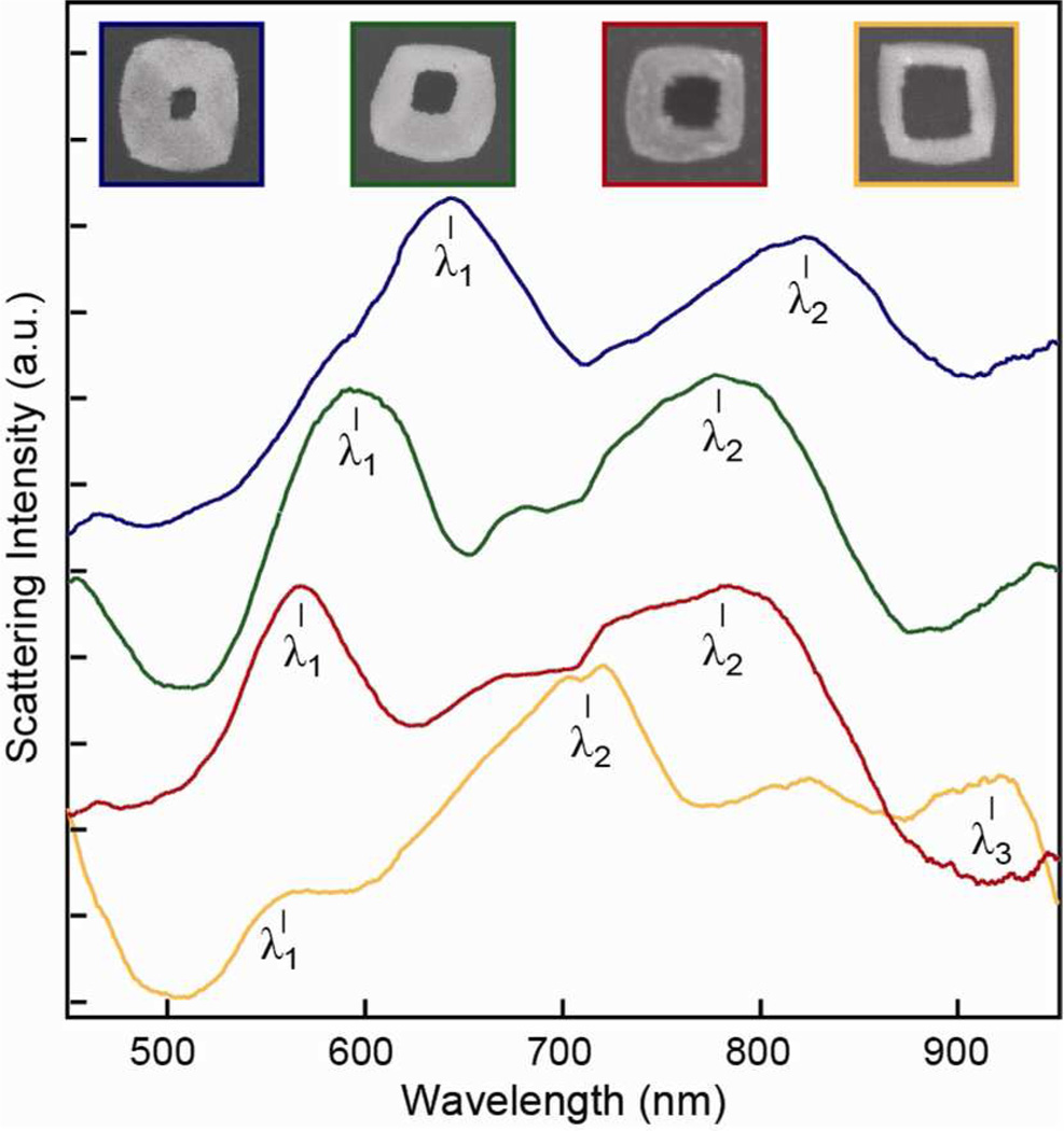
Tipless nanopyramids, pyramidal shells with an open, square hole instead of a sharp tip, can be fabricated from the same pyramidal Si template by depositing metal at an angle during the second E step of PEEL.33,13 The deposition angle determines the size of the hole and the height h of the tipless pyramids; these structural parameters are correlated. Single-particle spectroscopy showed a complicated spectral pattern with multiple plasmon resonances (db = 350 nm, t = 50 nm), and when h decreased (and hole size increased), two resonances in the spectra blue-shifted (Figure 5). Calculations by discrete dipole approximation (DDA) uncovered the nature of the peaks and revealed them to be hybrid bonding and anti-bonding modes between the inner and outer surfaces of the tipless shell. Systematic control of the hole size provides a different way to observe bonding and anti-bonding modes within a single multi-scale NP, compared with tuning shell thickness in Au nanoshells.13
Figure 5. Multi-scale 3D Au Tipless Nanopyramids exhibit Plasmon Resonances that Blue-Shift with Increased Truncation.
Single particle scattering of tipless nanopyramids (db = 350 nm, t = 50 nm) with larger tip openings (decreased heights). Resonances labeled λ1 and λ2 blue-shifted with increased truncation. (insets) SEM images of tipless particles that match the colored spectra. Images are 450 nm × 450 nm. Adapted with permission from ref. 13 © 2011 Wiley-VCH Verlag GmbH & Co. KGaA, Weinheim.
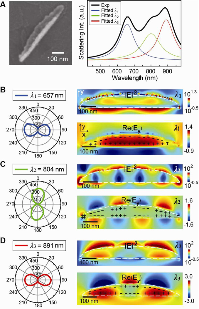
A final example of 3D, multi-scale particles that show unusual but characteristic near- and far-field properties are those with aspect ratios similar to the 1D rods discussed in Figure 2. Such structures can be accessed by changing the template base shape in PEEL, and they support multiple, multipolar plasmon resonances.8 Multi-scale Au particles with ARs ranging from 2.6 to 7.7 and a fixed width (120 nm) showed multiple LSP resonances between 420–980 nm.8 Each structure supported three different LSPs, designated λ1, λ2, and λ3, which exhibited identical trends in the polarization-dependent optical response. Figure 6 shows how scattering intensities of λ1 and λ3 were maximized when the incident light was polarized perpendicular to the long axis of the particle but that the scattering intensity at λ2 was the highest when the incident polarization was parallel to the long axis of the particle. Finite-difference time-domain (FDTD) modeling revealed that varying the length of the particles resulted in the excitation of a single multipolar longitudinal mode and two separate transverse modes with different multipolar orders (Figures 6B–D). Although increased multipolar orders for longitudinal modes have been reported for 1D rods,5, 6, 35 increased orders for the transverse plasmon resonances are not possible. Only in multi-scale, 3D anisotropic structures can two distinct transverse modes be observed.
Figure 6. Multi-scale Anisotropic Au NPs with High Aspect Ratios show Two Transverse Resonances.
FDTD calculations demonstrate that resolved resonances from measured scattering are multipolar, with the longitudinal mode at λ2, and two different transverse modes at λ1 and λ3. (A) SEM image and experimental and fitted single-particle spectra of a particle with aspect ratio = 6. (B–D) (left) Measured polarization-dependent scattering polar plots at λ1, λ2, and λ3. (upper right) Electric field intensity distributions at the respective plasmon wavelengths. (lower right) Charge distributions at each plasmon resonance. Adapted with permission from ref. 8 © (2012) American Chemical Society.
Multi-scale Plasmonic NPs and Hot Spot Volumes
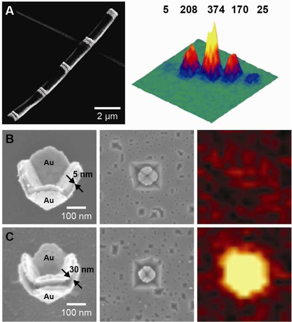
Besides providing a partial solution to the inverse problem, multi-scale plasmonic NPs offer opportunities in applications such as surface-enhanced Raman spectroscopy (SERS). Most work has focused on nanoscale (1–2 nm) gaps for optimized Raman enhancement25, 26, 32, 35–38 because the gap distances influence the intensity and distribution of the localized EM fields. Surprisingly, relatively large (10–30 nm) gap distances in coarse (>100 nm) length-scale particles have shown SERS signals comparable to NP substrates with gaps that were several nanometers (Figure 7).8,19 These particles were based on multi-scale 1D (nanorods) (Figure 7A) and 3D (nanopyramids) (Figure 7B) structures, where NP dimers were formed by depositing alternating layers of Au and a sacrificial metal within the template followed by etching of the spacer metal to produce well-defined gaps.
Figure 7. Multi-scale 1D and 3D SERS Active Particles.
(A) Fabricated nanorods with gaps of 160, 80, 30, 15 and 5 nm from top left to bottom right (right). 3D representation of a confocal Raman image. Reproduced with permission from ref. 36. © (2006) National Academy of Sciences, U.S.A. Pyramidal nanoshell dimers with (B) 5-nm gaps and (C) 30-nm gaps. Images from left to right show a particle released from the etched Si template, particles imbedded in the template, and a SERS image with dye and laser conditions similar to (A). Reproduced with permission from ref. 16. © (2010) American Chemical Society.
In addition, for 1D multi-scale rods, rough gaps led to SERS enhancements smaller than rods with smooth gaps.36 The reasons were that the roughness resulted in dephasing in the reflection of propagating from the gap, which weakened the resonances, and that more localized hot spots in the gap produced weaker coupling across the gap. Another unexpected characteristic of the 1D structures was that a periodic variation in SERS intensity was observed as a function of segment length. For the 3D multi-scale pyramids, as the gap g decreased, coupling between the inner and outer shells of the particle increased, which affected the plasmon resonance wavelength as well as the SERS response.16 Smaller gaps (g = 5 nm) produced a lower SERS response compared to larger gaps (g = 30 nm) (Figures 7B–C). This result is most likely from a combination of increased mismatch between the SERS excitation wavelength and the plasmon wavelength as well as improved near-field confinement from large (> 100 nm) particle sides at distances of tens of nanometers. Therefore, multi-scale plasmonic particles exhibit unique near-field and far-field properties that can result in 3D Raman-active volumes with characteristics different from smaller metal NP dimers.
In summary, we have presented examples of different multi-scale structures that support two or more length scales (fine, medium, coarse) and that show optical properties distinct from small, symmetric metal NPs. Such near-field and far-field properties, when compiled into a “plasmon resonance library,” provide a reasonable starting point for experimentally solving the inverse problem. Of course, the genetic algorithm method is also an emerging calculation tool that would be complementary. Regarding use of an optical library of resonances, if strong polarization-dependent properties were desired in perpendicular directions, where one resonance was in the visible and one was in the near to far-infrared, the particle should either be a multi-scale 1D rod or a 3D anisotropic particle. As further refinement, if instead of a single transverse mode, two transverse modes were needed, then the transverse direction must include multi-scale structure. As another example, if high local fields at mid-infrared wavelengths were wanted, then the Au particle should have at least one dimension >1000 nm and have sub-structure along that direction <10 nm; polarization criteria would further define the overall shape of the particle. A cataloguing of optical properties mapped to specific structural features is possible because of nanofabrication advances that enable flexibility in designing multi-scale plasmonic particles. Furthermore, although this Perspective highlighted how unexpected SERS responses can result from multi-scale structure in NP dimers, we anticipate that these unique geometrical features will have even broader impact in other applications, including nonlinear optics and optical imaging.
QUOTES TO HIGHLIGHT.
[M]ulti-scale NPs—structures with feature sizes that span three-orders of magnitude—offer a potential experimental solution to the inverse problem because they combine structure-function properties of both small and large metal particles.
Nanofabrication methods are an attractive approach not only for producing monodisperse particles reproducibly but also for controlling NP architecture at all three length-scale regimes (fine, medium, coarse), either independently or in combination as desired.
[M]ulti-scale plasmonic particles exhibit unique near-field and far-field properties that can result in 3D Raman-active volumes with characteristics different from smaller metal NP dimers.
A cataloguing of optical properties mapped to specific structural features is possible because of nanofabrication advances that enable flexibility in designing multi-scale plasmonic particles.
ACKNOWLEDGEMENTS
This work was supported by the National Science Foundation (NSF) under award number CHE-105801 (CMS, EY, TWO) and the NU-PSOC (NIH 1U54CA143869-01) (EY, TWO).
Biographies
Teri W. Odom is Board of Lady Managers of the Columbian Exposition Professor of Chemistry and Professor of Materials Science and Engineering at Northwestern University. She received her B.S. from Stanford University and her Ph.D. from Harvard University. Her research interests focus on controlling materials at the 100-nanometer scale and investigating their size and shape-dependent properties for applications in nano-optics, bio-imaging, and cancer therapeutics. http://chemgroups.northwestern.edu/odom/
Christina M. Sweeney received her Ph.D. in Chemistry at Northwestern University in 2011. She is currently a postdoctoral fellow at Northwestern studying the effects of surface-bound ligands on the ultrafast cooling dynamics of plasmonic nanoparticles.
Eun-Ah You received her Ph.D. in Chemistry at Northwestern University in 2012. She is currently a research scientist at LG Chemistry in Daejeon, Korea developing high performance thermoelectric materials by nanostructured design.
REFERENCES
- 1.El-Sayed MA, Link S. Spectral Properties and Relaxation Dynamics of Surface Plasmon Electronic Oscillations in Gold and Silver Nanodots and Nanorods. J Phys Chem B. 1999;103:8410–8426. [Google Scholar]
- 2.Schatz GC, Kelly KL, Coronado E, Zhao LL. The Optical Properties of Metal Nanoparticles: The Influence of Size, Shape, and Dielectric Environment. J Phys Chem B. 2003;107:668–677. [Google Scholar]
- 3.Noguez C. Surface Plasmons on Metal Nanoparticles: The Influence of Shpae and Physical Environment. J Phys Chem C. 2007;111:3806–3819. [Google Scholar]
- 4.Bohren CF, Huffman DR. Absorption and Scattering of Light by Small Particles. New York: Wiley; 1983. p. 530. p xiv. [Google Scholar]
- 5.Khlebtsov BN, Melnikov A, Khlebtsov NG. On the Extinction Multipole Plasmons in Gold Nanorods. J Quant Spectrosc Ra. 2007;107:306–314. [Google Scholar]
- 6.Payne EK, Shuford KL, Park S, Schatz GC, Mirkin CA. Multipole Plasmon Resonances in Gold Nanorods. J Phys Chem B. 2006;110:2150–2154. doi: 10.1021/jp056606x. [DOI] [PMC free article] [PubMed] [Google Scholar]
- 7.Felidj N, Grand J, Laurent G, Aubard J, Levi G, Hohenau A, Galler N, Aussenegg FR, Krenn JR. Multipolar Surface Plasmon Peaks on Gold Nanotriangles. J Chem Phys. 2008;128:094702. doi: 10.1063/1.2839273. [DOI] [PubMed] [Google Scholar]
- 8.You EZW, Suh JY, Huntington MD, Odom TW. Polarization-Dependent Multipolar Plasmon Resonances in Anisotropic Multiscale Au Particles. ACS Nano. 2012;6:1786–1794. doi: 10.1021/nn204845z. [DOI] [PMC free article] [PubMed] [Google Scholar]
- 9.Ross BM, Lee LP. Plasmon Tuning and Local Field Enhancement Maximization of the Nanocrescent. Nanotechnology. 2008;19:275201. doi: 10.1088/0957-4484/19/27/275201. [DOI] [PubMed] [Google Scholar]
- 10.Hao E, Schatz GC. Electromagnetic Fields around Silver Nanoparticles and Dimers. J Chem Phys. 2004;120:357–366. doi: 10.1063/1.1629280. [DOI] [PubMed] [Google Scholar]
- 11.Stoerzinger KA, Hasan W, Lin JY, Robles A, Odom TW. Screening Nanopyramid Assemblies to Optimize Surface Enhanced Raman Scattering. J Phys Chem Lett. 2010;1:1046–1050. doi: 10.1021/jz100095b. [DOI] [PMC free article] [PubMed] [Google Scholar]
- 12.Shuford KL, Lee J, Odom TW, Schatz GC. Optical Properties of Gold Pyramidal Shells. J Phys Chem C. 2008;112:6662–6666. [Google Scholar]
- 13.Sweeney CM, Stender CL, Nehl CL, Hasan W, Shuford KL, Odom TW. Optical Properties of Tipless Gold Nanopyramids. Small. 2011;7:2032–2036. doi: 10.1002/smll.201100758. [DOI] [PMC free article] [PubMed] [Google Scholar]
- 14.Atay T, Song JH, Nurmikko AV. Strongly Interacting Plasmon Nanoparticle Pairs: From Dipole-Dipole Interaction to Conductively Coupled Regime. Nano Lett. 2004;4:1627–1631. [Google Scholar]
- 15.Dmitriev A, Pakizeh T, Kall M, Sutherland DS. Gold-Silica-Gold Nanosandwiches: Tunable Bimodal Plasmonic Resonators. Small. 2007;3:294–299. doi: 10.1002/smll.200600409. [DOI] [PubMed] [Google Scholar]
- 16.Lin JY, Hasan W, Yang JC, Odom TW. Optical Properties of Nested Pyramidal Nanoshells. J Phys Chem C. 2010;114:7432–7435. doi: 10.1021/jp910627r. [DOI] [PMC free article] [PubMed] [Google Scholar]
- 17.Liao HW, Hafner JH. Monitoring Gold Nanorod Synthesis on Surfaces. J Phys Chem B. 2004;108:19276–19280. doi: 10.1021/jp061269t. [DOI] [PubMed] [Google Scholar]
- 18.Lee S, Mayer KM, Hafner JH. Improved Localized Surface Plasmon Resonance Immunoassay with Gold Bipyramid Substrates. Anal Chem. 2009;81:4450–4455. doi: 10.1021/ac900276n. [DOI] [PubMed] [Google Scholar]
- 19.Jana NR, Gearheart L, Murphy CJ. Seed-Mediated Growth Approach for Shape-Controlled Synthesis of Spheroidal and Rod-Like Gold Nanoparticles Using a Surfactant Template. Adv Mater. 2001;13:1389–1393. [Google Scholar]
- 20.Nehl CL, Liao HW, Hafner JH. Optical Properties of Star-Shaped Gold Nanoparticles. Nano Lett. 2006;6:683–688. doi: 10.1021/nl052409y. [DOI] [PubMed] [Google Scholar]
- 21.Oldenburg SJ, Averitt RD, Westcott SL, Halas NJ. Nanoengineering of Optical Resonances. Chem. Phys. Lett. 1998;288:243–247. [Google Scholar]
- 22.Foss CA, Hornyak GL, Stockert JA, Martin CR. Template-Synthesized Nanoscopic Gold Particles - Optical-Spectra and the Effects of Particle-Size and Shape. J Phys Chem-Us. 1994;98:2963–2971. [Google Scholar]
- 23.Ueno K, Mizeikis V, Juodkazis S, Sasaki K, Misawa H. Optical Properties of Nanoengineered Gold Blocks. Opt Lett. 2005;30:2158–2160. doi: 10.1364/ol.30.002158. [DOI] [PubMed] [Google Scholar]
- 24.Shumaker-Parry JS, Rochholz H, Kreiter M. Fabrication of Crescent-Shaped Optical Antennas. Adv Mater. 2005;17:2131–2138. [Google Scholar]
- 25.Henzie J, Kwak ES, Odom TW. Mesoscale Metallic Pyramids with Nanoscale Tips. Nano Lett. 2005;5:1199–1202. doi: 10.1021/nl0506148. [DOI] [PubMed] [Google Scholar]
- 26.Masuda H, Fukuda K. Ordered Metal Nanohole Arrays Made by a 2-Step Replication of Honeycomb Structures of Anodic Alumina. Science. 1995;268:1466–1468. doi: 10.1126/science.268.5216.1466. [DOI] [PubMed] [Google Scholar]
- 27.Almawlawi D, Liu CZ, Moskovits M. Nanowires Formed in Anodic Oxide Nanotemplates. J Mater Res. 1994;9:1014–1018. [Google Scholar]
- 28.Schmucker AL, Harris N, Banholzer MJ, Blaber MG, Osberg KD, Schatz GC, Mirkin CA. Correlating Nanorod Structure with Experimentally Measured and Theoretically Predicted Surface Plasmon Resonance. ACS Nano. 2010;4:5453–5463. doi: 10.1021/nn101493t. [DOI] [PubMed] [Google Scholar]
- 29.Biagioni P, Huang J-S, Hecht B. Nanoantennas for Visible and Infrared Radiation. Rep. on Prog. in Phys. 2012;75:024402. doi: 10.1088/0034-4885/75/2/024402. [DOI] [PubMed] [Google Scholar]
- 30.Bukasov R, Shumaker-Parry JS. Highly Tunable Infrared Extinction Properties of Gold Nanocrescents. Nano Lett. 2007;7:1113–1118. doi: 10.1021/nl062317o. [DOI] [PubMed] [Google Scholar]
- 31.Rochholz H, Bocchio N, Kreiter M. Tuning Resonances on Crescent-Shaped Noble-Metal Nanoparticles. New J Phys. 2007;9 [Google Scholar]
- 32.Lee J, Hasan W, Odomt TW. Tuning the Thickness and Orientation of Single Au Pyramids for Improved Refractive Index Sensitivities. J Phys Chem C. 2009;113:2205–2207. doi: 10.1021/jp8111155. [DOI] [PMC free article] [PubMed] [Google Scholar]
- 33.Lee J, Hasan W, Stender CL, Odom TW. Pyramids: A Platform for Designing Multifunctional Plasmonic Particles. Accounts Chem Res. 2008;41:1762–1771. doi: 10.1021/ar800126p. [DOI] [PubMed] [Google Scholar]
- 34.Hasan W, Lee JH, Henzie J, Odom TW. Selective Functionalization and Spectral Identification of Gold Nanopyramids. J Phys Chem C. 2007;111:17176–17179. [Google Scholar]
- 35.Encina ER, Coronado EA. Resonance Conditions for Multipole Plasmon Excitations in Noble Metal Nanorods. J Phys Chem C. 2007;111:16796–16801. [Google Scholar]
- 36.Qin L, Zou S, Xue C, Atkinson A, Schatz GC, Mirkin CA. Designing, Fabricating, and Imaging Raman Hot Spots. Proc. Nat. Acad. Sci. 2006;103:13300–13303. doi: 10.1073/pnas.0605889103. [DOI] [PMC free article] [PubMed] [Google Scholar]


