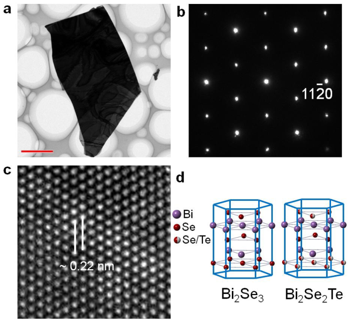
Figure 1. Structural characterization of cleaved flakes from Bi2Se2Te (BST) crystal.
(a) Low-magnification TEM image, (b) Selected area electron diffraction pattern, (c) High-resolution TEM (HRTEM) image of a BST flake on a holey carbon grid, respectively. The sharp SAED pattern in (b) indicates the high-quality single crystal. The HRTEM image in (c) reveals a perfect crystalline structure and the spacing between the  atomic planes is resolved to be 0.22 nm (marked by a pair of parallel lines). (d) Layered crystal structure of Bi2Se3 and Bi2Se2Te, showing the disordered occupation of Se/Te atoms in outer quintuple layers. Scale bars in (a) is 2 μm.

