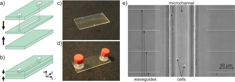
Fig. 2.
Schematic representation of the microfluidic chip fabrication technique: a) three-layer technology with the central fused silica glass slide machined by femtosecond lasers and b) sealing of the channel with two polished glass slides. Image of the microfluidic chip c) without and d) with fluidic connections to the straight microchannel. e) Phase contrast microscope picture of femtosecond-laser-written optical waveguides integrated in the microfluidic chip facing the channel to create the MOS.

