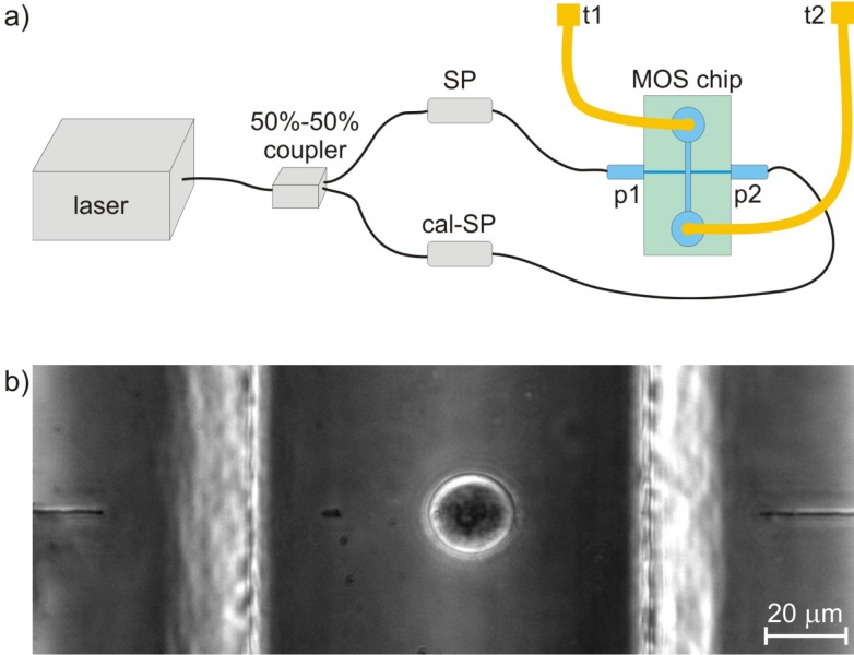
Fig. 3.
(a) Schematic representation of the experimental setup for the MOS device: ‘SP’ indicates the fused splice, while ‘cal-SP’ indicates the splice used for trap calibration; ‘t1’ and ‘t2’ indicate the two PEEK tubing terminations; ‘p1’ and ‘p2’ are the two fibre pigtails. (b) Phase contrast microscope image of an HL60 cell trapped in the MOS; optical waveguides are also visible at the two sides.

