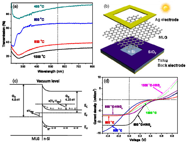
Figure 3 .
Optical transmission spectra, solar cell device configuration, energy band diagram, and light current density-voltage curves. (a) Optical transmission spectra of samples produced at different temperatures. (b) Schematic diagram of the solar cell device configuration. (c) The energy band diagram of the forward-biased MLG/n-Si junction upon illumination. ΦG and ΦSi is the work function of MLG and n-Si, respectively. V0 is the built-in potential, and Vbias is the applied voltage. The photogenerated holes (h+) and electrons (e−) are driven by V0 into the MLG and n-Si, respectively. (d) Light current density-voltage curves of the solar cells based on 600°C, 800°C, and 1,000°C samples, and the corresponding cells after HNO3 treatment.

