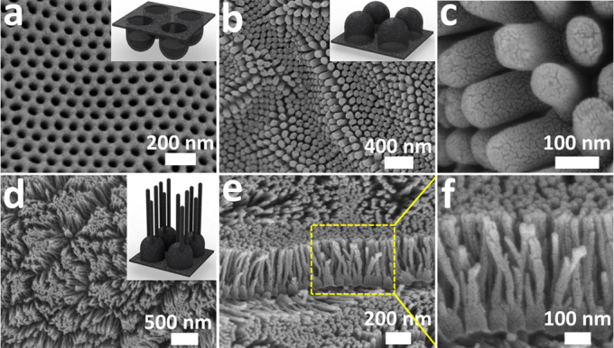
Figure 1. SEM images of CNCs.

SEM images of (a) concave and (b, c) convex and (d–f) branched nanocup films. (c) is high magnification SEM image of (b) convex nanocup with 80±10 nm in diameter and 140±10 nm in length. (e, f) is cross-sectional view of (d) branched nanocup film and (f) is high magnification image of (e), where short carbon nanotubes (25 nm in diameter and 330±10 nm in length) are branched from the bottom of a nanocup. Note that the thickness of CNCs film can be controlled by changing carbon deposition time or carbon concentration during a CVD process. The inset figures show schematics of concave, convex and branched convex nanocup film.
