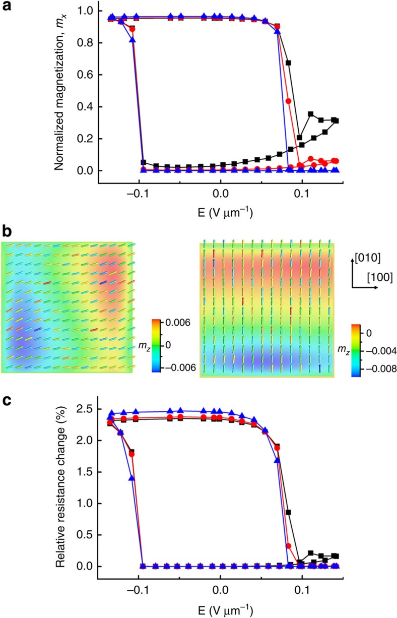
Figure 2. Thickness-dependent switching behaviour.
(a) Electric-field-induced magnetization rotation in the Ni-free layers with thicknesses of 35 nm (squares), 15 nm (circles) and 5 nm (triangles), respectively. mx indicates the the normalized magnetization in the in-plane [100] direction. The lateral size (length and width) is set as 64 nm. (b) Vector diagrams of the bistable magnetization distributions at E=0, that is, mx=0.9538 (left) and 0.0364 (right), in the 64×64×35 nm3 Ni-free layer. (colour bar) mz indicates the normalized magnetization in the out-of-plane [001] direction. (c) Hysteric loops of relative device resistance change upon the perpendicular electric fields applied to the (011) PMN-PT layer, accompanied with the magnetization switching in the Ni-free layers with thicknesses of 35 nm (squares), 15 nm (circles) and 5 nm (triangles), respectively.

