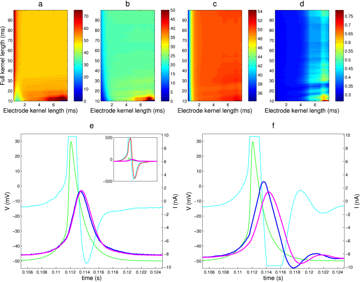
Fig. 4.
Demonstration of artifact compensation on a model cell. (a–d) AEC estimated circuit properties obtained from electrode calibration for a wide region of AEC's two crucial parameters (full kernel length and electrode kernel length, see Brette et al. (2008) for details). There is a large area in this parameter region where the true resistances and time constants are recovered correctly. (e–f) Comparison of AEC and bridge balance compensation for simulating a 500 nS gap junction (electrical synapse) from a simulated cell (spike generator) to the (physical) model cell. (e) Retrieved membrane potential using AEC and the AEC calculated electrode artifact (inset). (f) Results of using bridge balance compensation. Colour code: green: spike generator potential, cyan: injected current, red: calculated electrode artifact (Ve), magenta: calculated membrane potential (Vraw − Ve) in case of AEC (e), amplifier provided measurement of the membrane potential in case of bridge balance (g), blue: control (“true”) membrane potential on a separate channel. The bridge balance compensated signal is delayed and exhibits artifactual damped oscillations. This is a good example of how the errors in compensation are fed back into the system during dynamic clamp, leading to marked differences in the entire system's behavior. Model cell properties: model electrode: Re = 50 MΩ, τe = 0.35 ms, model membrane: Rm = 50 MΩ, τm = 23 ms.

