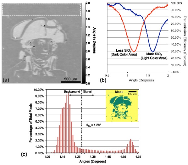
Fig. 4.

(a) Label-free image of the PC with a pattern of deposited 10 nm SiO2 film. The image clearly highlights the variation in resonance angle in the transparent and opaque areas of the pattern Our selection of a negative control region is highlighted with a white dashed box. (b) Transmission spectrum of the pattern showing the difference in angle of resonance (minima in transmission) for the areas with and without additional SiO2. More SiO2 gives a larger resonance angle. (c) Histogram showing the distribution of resonance angle versus the number of pixels used to make our selection of the threshold angle. The inset image shows the mask generated by using the threshold set by θTA = 1.28 °. The green region has a resonance angle above the threshold angle and the yellow region has a resonance angle below the threshold angle.
