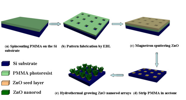
Figure 1.

Schematics of the experimental procedures of patterned ZnO nanorod arrays. (a) Spincoating PMMA on Si substrate; (b) Pattern fabrication by EBL method; (c) Magnetron sputtering ZnO seed layer; (d) Strip PMMA in acetone solution; (e) Hydrothermal growth ZnO nanorods on the patterned areas.
