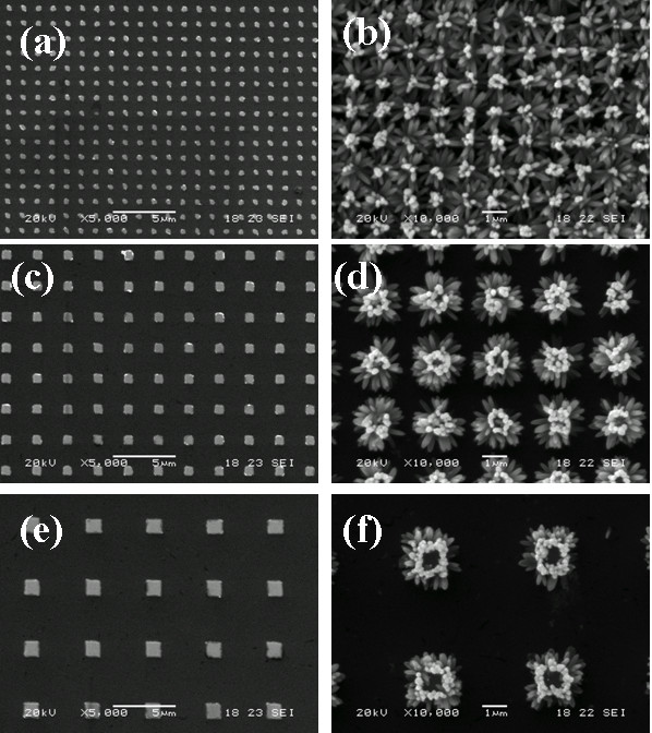
Figure 2.

The SEM image of ZnO dot area and nanorod arrays. (a) The SEM image of ZnO dot area with 200 × 200 nm; (c) dot area is 500 × 500 nm; and (e) dot area is 1 × 1 μm. (b) The SEM image of ZnO nanorod arrays with 1-h hydrothermal reaction process on 200 × 200 nm seed areas; (d) on 500 × 500 nm seed areas; and (f) on 1 × 1 μm seed areas.
