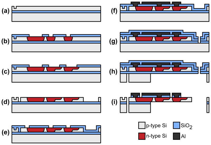
Figure 3.
Fabrication process. (a) Alignment marks are patterned and etched. (b) The wafers are oxidized, coated with additional LTO and annealed. Windows are opened in the oxide mask and the contacts are POCl3 doped at 900°C. (c) The oxide windows are opened further and the piezoresistors are POCl3 doped at 825°C. (d) The oxide is stripped and the device layer is patterned and etched via reactive ion etching (RIE). (e) A layer of LTO is deposited and vias are opened. (f) The wafer is metallized and etched back via RIE. (g) An additional layer of LTO is deposited and cracks are patterned into the oxide stack. (h) The backside of the SOI wafer is patterned, a carrier wafer is bonded to the frontside, the backside is etched via DRIE, and the SOI wafer is debonded. (i) The BOX and LTO layers are etched via vapor HF in order to release the probes.

