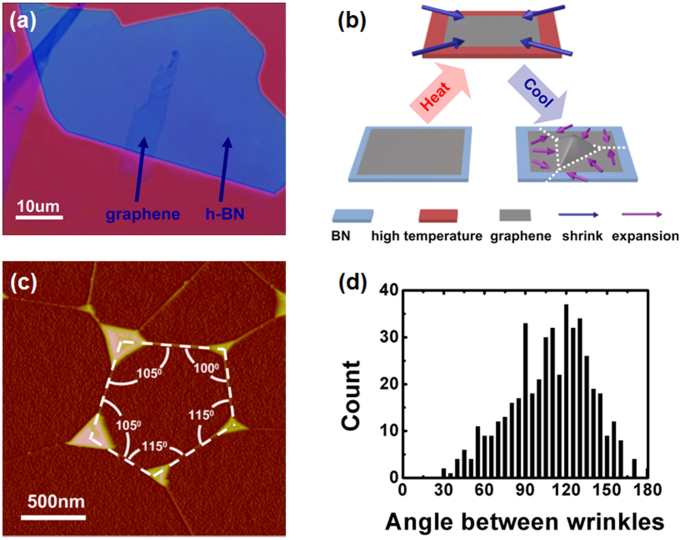
Figure 1.
(a) Optical image of a single-layer GBN sample on 300nm SiO2. (b) Schematics of the proposed formation process of graphene bubbles and ridges on BN. (c) A representative AFM image of GBN bubbles and ridges after thermal annealing. Angles between the adjacent ridges are indicated. (d) Distribution of the angles between neighboring ridges showing a peak around 120 degree.

