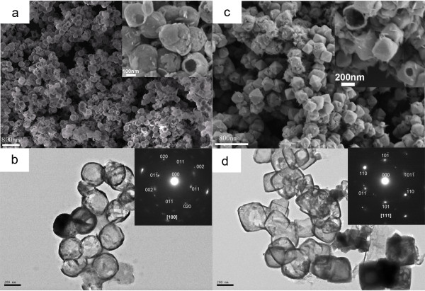
Figure 1.
SEM and TEM images of hollow Cu2O samples. (a, b) SEM and TEM images of spherical Cu2O (SI1-A1 in Additional file 1), (c, d) SEM and TEM images of octahedral Cu2O (SI1-A2 in Additional file 1). The inset of (a) and (c) are the corresponding enlarged views of hollow Cu2O samples. The inset of (b) and (d) are the corresponding SAED patterns of the Cu2O samples.

