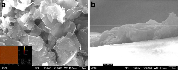
Figure 3.

SEM and AFM images of typical graphene-on-silicon devices. SEM top view (a) and cross section view (b) images of the typical graphene-on-silicon devices. The inset in (a) displays the AFM image of the graphene flakes obtained from the supernatant.
