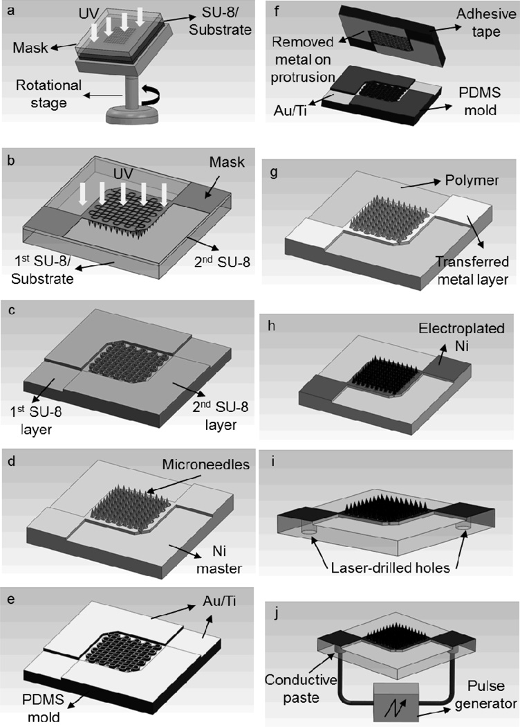
Figure 7.
Schematic illustration of the fabrication process for an electroporation microneedle array: (a) inclined UV exposure of the first SU-8 layer to form an inverse shape of microneedles, (b) UV exposure of the second SU-8 layer to form protrusion structures, (c) formation of a two-layer SU-8 mold by dissolving uncrosslinked SU-8 in PGMEA (refer to Figures 1a and 1b), (d) master structure formation by electrodeposition of nickel into the SU-8 mold and separation from the mold (refer to Figure 1c), (e) metal deposition on the PDMS mold replicated from the master, (f) removal of metal on the protrusion of the PDMS mold (refer to Figure 1d), (g) replication of metal-patterned polymer microneedle array from the PDMS mold by metal transfer micromolding (refer to Figures 1e and 1f), (h) Ni electroplating on the microneedle array (refer to Figure 1g), (i) formation of micro-vias from the backside using laser drilling, and (j) conductive polymer filling into the micro-vias and formation of electrical connection to the outer electronics (refer to Figure 1h).

