Figure 1.
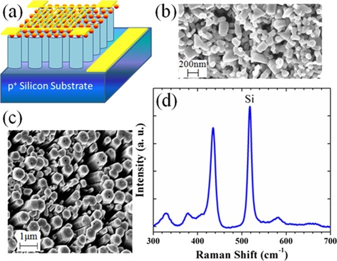
(a) 3D view of heterojunction photodiode fabricated from ZnO NWs grown on top of p-Si substrates. (b) A SEM image showing the morphology of the PVA coated ZnO nanoparticles on top of the ZnO NWs and (c) hydrogen treated ZnO NWs on top of p-Si substrates. (d) Raman spectra of the hydrogen treated ZnO NWs on top of p-Si substrate.

