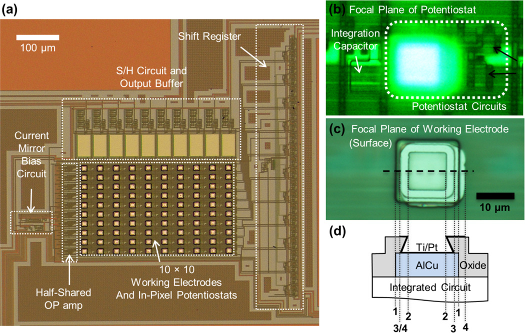
Fig. 1.
Amperometric amplifier array. (a) Photograph of chip surface with working electrodes and underlying circuitry after post-fabrication. The 10 × 10 electrode array was visible as bright squares; each electrode was 15 µm × 15 µm in size. Each in-pixel potentiostat contains only a half of an operational amplifier taking advantage of a half-shared operational amplifier design. The shift register controlled the timing of the S/H circuit to multiplex the electrode outputs per each column of 10 electrodes. (b) and (c) are microphotographs of individual electrode /potentiostat array element at different focal planes. The focal plane of (b) was at the underlying potentiostat, consisting of 9 transistors (two of which are indicated by black arrows) and an integrating capacitor that converted the recording current to voltage. The focal plane of (c) was at the surface working electrode above the potentiostat. (d) Schematic of electrode topology. 15 µm × 15 µm AlCu contacts served as interconnection between the surface patterned Pt electrode and the potentiostat. The overglass has 10 µm ×10 µm openings at the top with an undercut expanding to a ~12 µm × 12 µm area of exposed AlCu. The thick black line, atop AlCu and Oxide, indicates the area covered by Ti/Pt. The cross section along the horizontal dashed line is shown schematically in (c). The vertical dotted lines indicate the edges of the AlCu contacts (1), the overglass opening (2), the undercut (3), and the slightly misaligned bright area where Pt is patterned (4).

