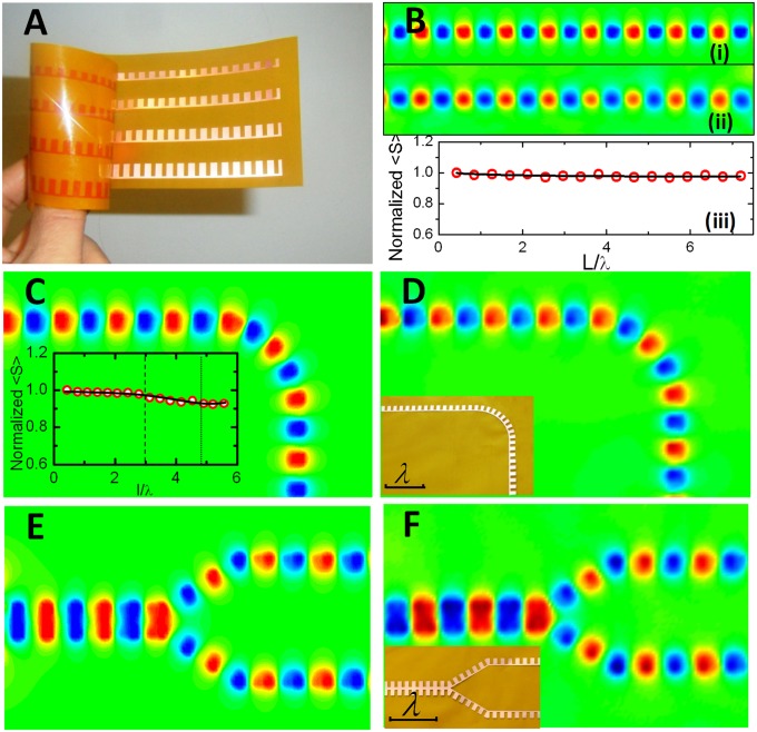
Fig. 3.
Simulation and measurement results of CSP waves on planar surfaces at 10 GHz. (A) Photograph of the nearly zero-thickness CSP structures on a flexible and ultrathin dielectric film, which can be wrapped on arbitrarily curved surfaces. The four CSP strips shown have groove depths h, from top to bottom, of 3, 4, 5, and 6 mm. Here a = 2 mm, d = 5 mm, t = 0.018 mm, and W = h + 1 mm. (B) Simulation (i) and measurement (ii) results of electric field (Ez) distributions along the ultrathin corrugated metal strip with groove depth h = 3 mm. (iii) Normalized time-averaged power densities (peak values) along an observation line (l) lying 1.5 mm above the corrugated edge. (C and D) Simulated (C) and measured (D) electric fields (Ez) of the 90o bend. (C, Inset) Normalized time-averaged power densities (peak values) along a bending observation line (l) lying 1.5 mm above the corrugated edge, in which the region between two thin dashed lines is the bending path. (D, Inset) Photograph of an experimental sample, with a = 2 mm, d = 5 mm, h = 4 mm, W = 5 mm, and t = 0.018 mm. (E and F) Simulated (E) and measured (F) electric fields (Ez) of the 60o Y-splitter. (F, Inset) Photograph of an experimental sample, with a = 2 mm, d = 5 mm, h = 4 mm, W = 5 mm, and t = 0.018 mm. In all cases, an electric monopole parallel to the plane was used to excite the CSP modes at the left edge.

