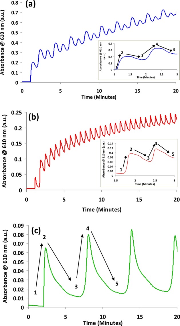
Figure 5.

(a–c) Changes in absorbance at 610 nm for platform I as a function of potential window and the incident scan rate ((a) voltage window, +/– 3 V; scan rate, 100 mV/s; (b) +/– 2 V, 100 mV/s; and (c) +/– 1.75 V, 10 mV/s.) The insets in parts a and b show magnified portions of the scans for the time sections indicated on the axis.
