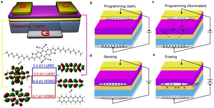
Figure 1. Schematic diagram and operational principle of LCOM.
(a) Device configuration of LCOM and the molecular structures of materials used as semiconductor and charge storage layer. HOMO-LUMO energy levels and electronic structures are determined by density functional theory calculations at the B3LYP/6-31G(d) level of theory. The device uses silica as dielectric layer (300 nm). Source−Drain electrodes are made of gold while heavily doped silicon as gate electrode. Electrical field assisted electron injection from pentacene into memory layer as the device is: (b) In dark. (c) Illuminated. The photo-excited electrons in pentacene would transport into the memory layer and stay there. (d) Device operated in TFT mode as holes accumulate at the pentacene/M-C10 interface. (e) Electric field assisted hole injection from pentacene into M-C10 when the gate voltage is enough negative. This could be recognized as an erasing process.

