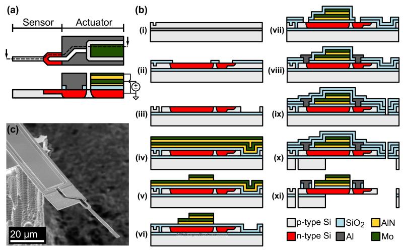
Figure 1.
Force probe layout, fabrication process and example device. (a) The probe consists of a narrow, soft piezoresistive sensor attached to the end of a wide, stiff piezoelectric actuator. Placement of the actuator at the base enables larger tip deflections, higher bandwidth operation and decouples the mechanical design of the actuator and sensor. (b) The probes are fabricated from SOI wafers in a nine-mask process via optical lithography. (c) SEM of a finished device. The sensor is 300 nm thick, 2 μm wide and 45 μm long with a 5.9 μm long piezoresistor while the actuator is 50 μm long and 20 μm wide.

