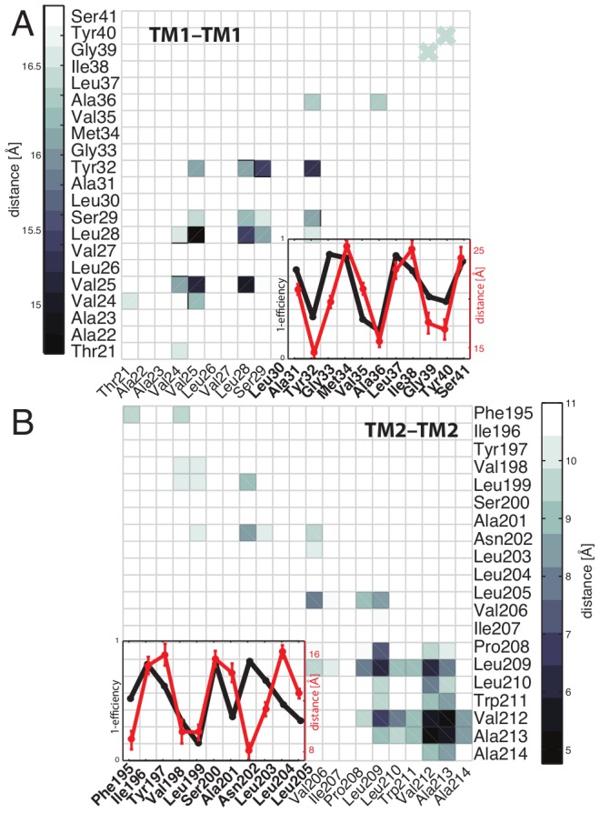
Figure 3. TM structural validation using disulfide cross-linking scanning.

MD-averaged contact maps for (A) TM1 and (B) TM2 interfaces within the assembled TM domain. A direct comparison with cross-linking efficiency of (A) TM1 and (B) TM2 is reported in the inset, and shows a strong correlation between the cross-linking (1-efficiency) (in black) and the MD-averaged Cα distance measured for the TM model structure (in red). The cross-linking efficiency for the whole TM1 and TM2 regions is reported in Figure S1.
