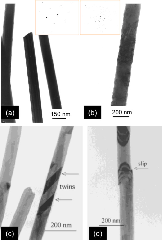
Figure 7.
TEM images of representative Cu nanowires and lattice defects: (a) single-crystalline and (b) polycrystalline Cu wires together with their corresponding SAED patterns (insets). (c) 70 nm diameter single-crystalline wire with twin structures. (d) Slip in a 100 nm diameter Cu wire. (a,b) Adapted with permission from [71] – Copyright 2001 Elsevier and (c,d) adapted with permission from [52] – Copyright 2001 Wiley-VCH.

