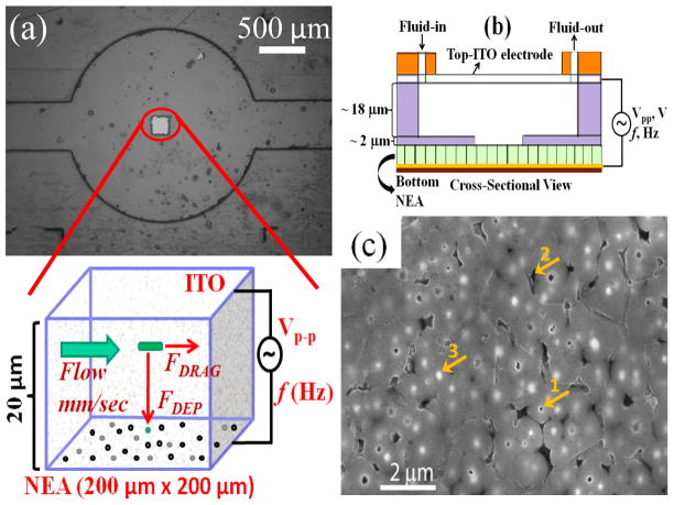
Figure 1.
Design of nano-DEP device. (a) A brightfield image of a nano-DEP device. The small square (200 μm × 200 μm) at the center is the exposed active CNF NEA placed at the bottom. The inset beneath shows the enlarged schematic of an E. coli cell influenced by the major forces when it flows through the channel between the two electrodes where a AC voltage is applied. The total height of the channel is 20 μm. (b) Cross-sectional schematic view of the nano-DEP-device. (c) A SEM image (top view) of the CNF NEA with arrow 1 indicating an exposed CNF tip, arrow 2 as a void in SiO2 matrix, and arrow 3 for unexposed CNF tip.

