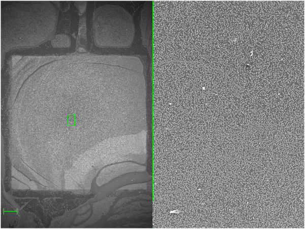
Figure 4.

Semi-covered layer of scattered nanospheres. SEM pictures showing a monolayer of 360-nm polystyrene nanospheres deposited under the conditions shown in the eighth row of Table 1. The semi-covered monolayer follows the patterned contact, a squared electrode in the center of the left image and a path for electrical conduction at the top. Scale bar is 200 μm.
