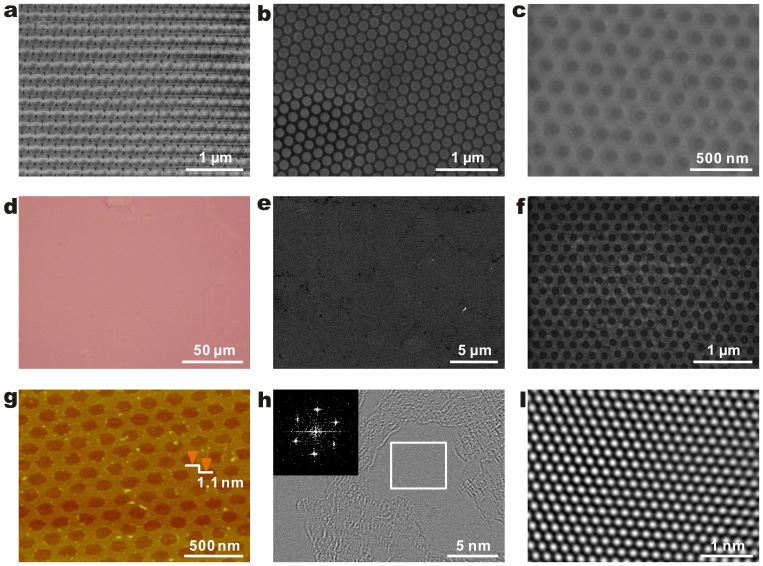
Figure 2. Morphology and structure characterization of as-grown GNM.
(a) SEM image of the close-packed monolayer of PS nanosphere with the diameter of 230 nm. (b) SEM image of PS nanosphere with ~40 nm gap after O2 plasma etching. (c) SEM image of periodic SiO2 mask on Cu foil after CF4 plasma etching of the exposed SiO2 and removing of PS nanosphere. (d) OM image of the large-area and homogeneous GNM on Si substrate with 300 nm SiO2 after graphene growth on patterned Cu foil, removing of SiO2 mask and the transfer of sample. (e) Low-magnification SEM image of the as-grown GNM showing the existence of boundary line resulted from the configuration of PS nanosphere film. (f) High-magnification SEM image of the GNM morphology. (g) AFM image of GNM structure with the thickness of ~1.1 nm except some PMMA residues from transfer process. (h) AC-HRTEM image and the corresponding Fourier transform of the single-crystal GNM neck. (i) Fourier enhanced TEM micrograph of the marked area in (h) showing a single set of a hexagonal spot pattern.

