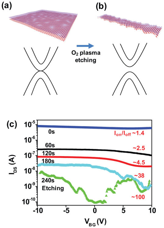
Figure 2. The opening of transport gap in bilayer graphene by narrowing channel width.

(a–b), Schematic images of (a), bilayer graphene sheet and (b), bilayer graphene nanoribbon with corresponding band diagrams. (c), Transfer characteristics of a bilayer GNR FET at the various oxygen plasma etching time (VDS = 0.1 V). The etching time was varied from 0 s to 240 s from top to bottom in steps of 60 s.
