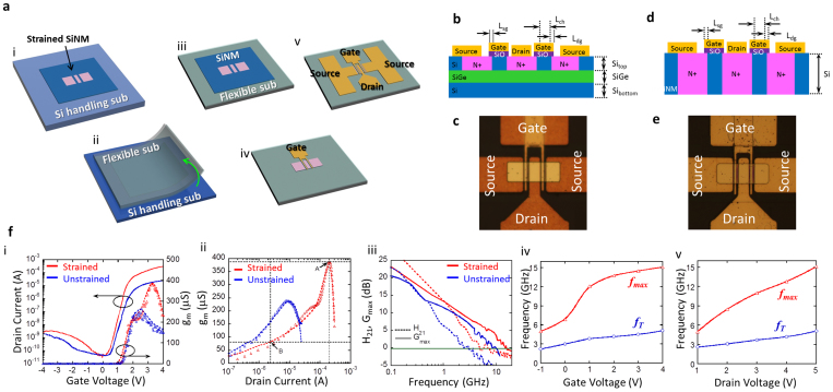
Figure 3. Device fabrication on released strained Si/SiGe/Si NMs and characterizations.
(a), Process flow for device fabrication. i, Released strained NM sitting on handling substrate. ii–iii, NM is flip transferred to a PET substrate. iv, Gate stack formation using lift-off techniques. v, Source/drain and a interconnect spelling-metallization. (b), Cross sectional illustration of strained-NM device dimensions. (c), Optical image of a fabricated strained device. (d), Cross sectional illustration of unstrained device dimensions. (e), Optical image of a fabricated unstrained device. For both strained and unstrained devices, the gate lengths (Lg = Lch+Lsg+Ldg) is 2.5 μm and gate width is 40 μm. Having a gate overlap distance with source/drain regions (Lsg and Ldg) of 0.5 μm, the effective channel lengths (Lch) are 1.5 μm. (f), Device DC and RF response characteristics of unstrained and strained devices. i, Transfer curves and calculated transconductance (gm) curves of unstrained and strained devices (Vds = 500 mV). ii, gm is plotted as a function of drain current. Point A indicates the peak gm where peak fT/fmax values were measured. Point B is where 3.5 GHz fmax can be obtained. The drain current at point B is roughly two orders lower than that at point A. iii, Current gain (H21) and power gain (Gmax) as a function of frequency of unstrained and strained devices (Vg = 4 V, Vds = 5 V). iv and v, fT and fmax of strained devices as a function of gate bias under fixed drain bias (Vds = 5 V) and that as a function of drain bias under fixed gate bias (Vg = 4 V), respectively.

