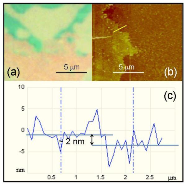
Figure 1.
Optical and AFM images of CVD-grown graphene used in our work. (a) Optical image of an edge of graphene layer transferred to Si/ 300 nm SiO2 substrate. The purple color corresponds to uncovered substrate, the light green-blue color corresponds to the thinner, major part of graphene, and the darker green “islands” show the areas where the next layer of graphene started to grow. (b) AFM image of one of edges of CVD-grown graphene transferred to Si/SiO2. Bright yellow line shows the direction of profile “cut” show in (c). (c) The AFM thickness profile of the edge of graphene shown in (b). Despite of the ocsillations caused the inherent roughness of the CVD-grown SiO2 layer, we see the thickness of graphene of about 2 nm.

