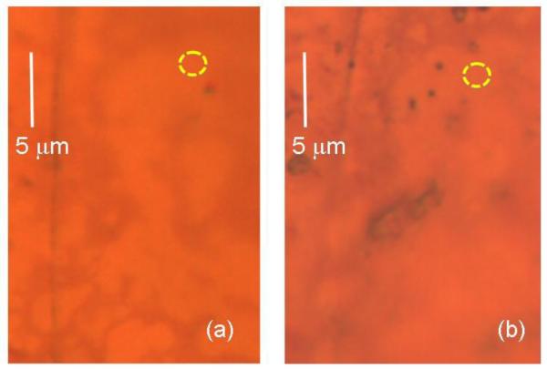
Figure 3.
Optical images of the selected area of CVD-grown graphene on Cu substrate (a) before and (b) after 8 days of chemical treatment with TMST and CsF. The yellow dashed line encircled area shows the place from which we collected the Raman spectra shown in the Figure 4.

