
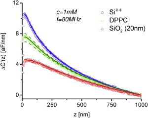
Figure 4.
Experimental capacitance gradient approach curves (symbols) measured onto the Si++ substrate (circles), the SiO2 stripe (triangles), and the DPPC patch (squares) at the locations indicated by symbols in Fig. 3e. The applied voltage was v0 = 0.25 V, the frequency f = 80 MHz, and the concentration 1 mM. (Solid lines) Finite element numerical simulations of the tip-sample system with dielectric constants εr,SiO2 = 4 and εr,DPPC = 3.2, for SiO2 and DPPC, respectively. In the calculations we used a tip radius R = 45 nm, a cone angle θ = 15°, and a native oxide capacitance Cnative = 0.71 μF/cm2 obtained by fitting the numerical calculations to the force curve on the Si++ substrate (solid line). (Dashed lines) Simulations for εr,DPPC = 2.2 and 4.2. Additional model parameters used in the numerical calculations: oxide/lipid heights and radii: hSiO2 = 20 nm; lSiO2 = 1.5 μm; hDPPC = 5 nm; lDPPC = 0.75 μm; and cone height H = 10 μm. The data are presented with ΔC′(z = 1000 nm) set to zero.