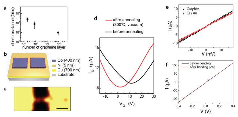
Figure 2. Synthesis and electrical characteristics of monolithic graphene-graphite backgate FETs.
a, Sheet resistance as a function of the number of the graphene layers (n). The error bars represent one standard deviation. b, Schematic illustration of the catalyst pattern to synthesize the monolithic FET. Red-dashed lines indicate the masked area against O2 plasma etching for device isolation after the CVD synthesis. c, Raman map (G band) of the graphene channel area with graphitic source/drain after the isolation step (channel width: 1 μm, length: 4 μm). Scale bar, 5 μm. d, ID-VG characteristics of monolithic graphene-graphite backgate FET (VD: 0.1 V). e, Comparison of contact properties (i) between the monolithic graphene channel and graphite electrodes (black square) and (ii) between graphene and the Cr (2 nm) / Au (100 nm) electrodes evaporated on graphene (red), with the identical dimensions of electrode pads and the channel. f, Electrical characterization (I-V) of graphite electrode before and after elastic bending/distortion (strain of ~2%). Thickness of graphite electrodes in Fig. 2c-2f is ~300 ± 63 nm.

