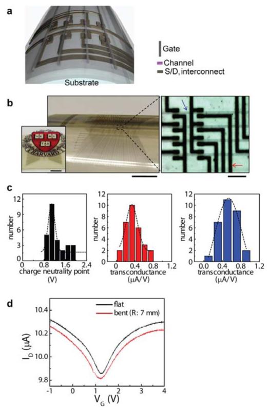
Figure 4. Flexible and semitransparent topgate monolithic graphene-graphite FET arrays.
a, Schematic illustration of the device layout. b, Photograph (main panel) of the devices wrapped on a cylindrical glass (radius of curvature: 1.2 cm). The device rested on a paper printed with a logo, to demonstrate the semitransparent characteristics of the monolithic graphene-graphite devices (left inset). Scale bars, 4 mm. Optical micrograph of the topgate FET arrays (right image). Scale bar, 200 μm. The blue arrow presents the topgate line, and the red arrow indicates the S/D with interconnects. c, Statistic distributions of charge neutrality point (left panel) and transconductance at n-(center) and p- (right) type regimes. d, ID-VG curve of the topgate FET measured when the substrate is flat and bent (radius of curvature: 0.7 cm).

