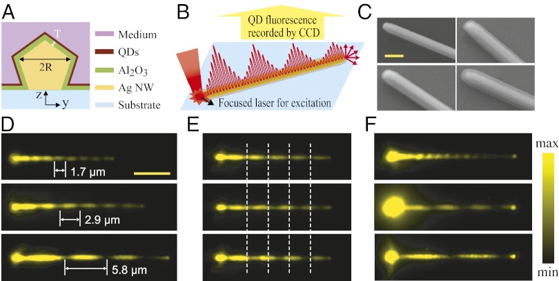
Fig. 1.
Near-field distribution images for NWs with different dielectric environments. (A) Schematic cross-section of the samples. (B) Schematic illustration of the excitation/collection configuration and the plasmons propagating along the NW. (C) SEM images of a typical bare Ag NW (Upper Left) and NWs coated with T = 30 nm (Lower Left), 50 nm (Upper Right), and 80 nm (Lower Right) Al2O3 layers. (Scale bar, 500 nm.) (D) QD emission images under excitation at the left ends of the NWs. From Top to Bottom, the radius of the NWs is 160, 155, and 157 nm, and the corresponding Al2O3 thicknesses are 30, 50, and 80 nm. (E) QD emission images for a 162-nm radius NW with a 50-nm Al2O3 coating measured in air (Top), and then after depositing 5 nm of Al2O3 (Middle), and finally with an additional 5 nm of Al2O3 (Bottom). The white dashed lines are visual guides to show the shift of the plasmon near-field pattern. (F) QD emission images for a 155-nm radius NW initially coated with 10 nm of Al2O3 and QDs, and then capped with another 5 nm of Al2O3 to protect the water-soluble QDs from being removed, measured in air (Top), water (Middle), and oil (Bottom). (Scale bar in D for D–F, 5 µm.)

